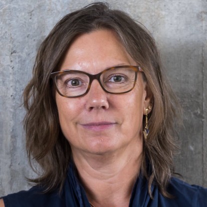
Helga Janning
Contact
janning@wib.tu-...
work +49 6151 16-22266
fax +49 6151 16-22211
Work
L2|08 108
El-Lissitzky-Str. 4
64287
Darmstadt
Helga Janning was born in Meppen Germany.
In 1989 she got her graduation as Physics-Technicial Assistent at the Technische Unterrichtsanstalten der Stadt Mülheim (Ruhr).
From 1989 – 2007 she worked in the research and development of III/V semiconductor devices for telecommunication purpose. Various kinds of Laser Diodes were developed and her special focus was the technology, the epitaxial (re)growth, characterisation and the analysis of materials and devices. A main tool for these investigations was always the field emission electron microscope.
Between 2007 and 2013 the interests on semiconductors widened to the investigations on the fatigue of different OLED materials with the SFB 595 at the Materials Sciences dept. of the TU-Darmstadt in the working group “Electronic Materials”.
2013-2018 still in the Materials Science dept., Helga worked on synthesis, measurement and characterisation of different magnetic materials. Managing the labs and the work safety were of her deep interest.
Since 2018 she brings her expertise on Electron Microscopy and micro-range analysis to the Institut für Werkstoffe im Bauwesen into the Fachbereich 13.


